- 您现在的位置:买卖IC网 > Sheet目录531 > UPG2185T6R-E2-A (CEL)IC SW SPDT 2GHZ-6GHZ 6-TSSON
�� �
�
�A� Business� Partner� of� Renesas� Electronics� Corporation.�
�μ� PG2185T6R�
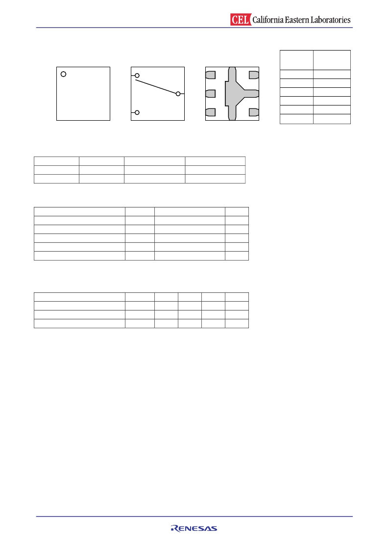
�PIN� CONNECTIONS� AND� INTERNAL� BLOCK� DIAGRAM�
�(Top� View)�
�(Top� View)�
�(Bottom� View)�
�Pin� No.�
�Pin� Name�
�1�
�6�
�1�
�6�
�6�
�1�
�1�
�OUTPUT1�
�2�
�GND�
�2�
�5�
�2�
�5�
�5�
�2�
�3�
�OUTPUT2�
�4�
�V� cont� 2�
�3�
�4�
�3�
�4�
�4�
�3�
�5�
�INPUT�
�6�
�V� cont� 1�
�Remark� Exposed� pad� :� GND�
�TRUTH� TABLE�
�V� cont� 1�
�High�
�Low�
�V� cont� 2�
�Low�
�High�
�INPUT� ?� OUTPUT1�
�OFF�
�ON�
�INPUT� ?� OUTPUT2�
�ON�
�OFF�
�ABSOLUTE� MAXIMUM� RATINGS� (T� A� =� +25� °� C,� unless� otherwise� specified)�
�Parameter�
�Symbol�
�Ratings�
�Unit�
�Switch� Control� Voltage�
�V� cont�
�+6.0�
�Note�
�V�
�Input� Power�
�Power� Dissipation�
�Operating� Ambient� Temperature�
�Storage� Temperature�
�?� V� cont� 1� ?� V� cont� 2� ?� ≤� 6.0� V�
�Note:�
�P� in�
�P� D�
�T� A�
�T� stg�
�+31�
�150�
�?� 40� to� +90�
�?� 55� to� +150�
�dBm�
�mW�
�°� C�
�°� C�
�RECOMMENDED� OPERATING� RANGE� (T� A� =� +25� °� C,� unless� otherwise� specified)�
�Parameter�
�Symbol�
�MIN.�
�TYP.�
�MAX.�
�Unit�
�<R>�
�Switch� Control� Voltage� (H)�
�Switch� Control� Voltage� (L)�
�Operating� Frequency�
�V� cont� (H)�
�V� cont� (L)�
�f�
�1.8�
�?� 0.2�
�2.0�
�3.0�
�0�
�?�
�3.6�
�+0.2�
�6.0�
�V�
�V�
�GHz�
�R09DS0053EJ0300� Rev.3.00�
�Nov� 22,� 2012�
�Page� 2� of� 9�
�发布紧急采购,3分钟左右您将得到回复。
相关PDF资料
UPG2189TB-A
IC SW SPST 6-MINIMOLD
UPG2214TB-E4-A
IC SWITCH SPDT 6-SMINI
UPG2214TK-EVAL-A
EVAL BOARD FOR UPG2214TK
UPG2250T5N-A
GAAS MMIC BLUETOOTH-ZIGB 6TSON
UPG2251T6M-E2-A
IC AMP BLUETOOTH 12TSQFN
UPG2253T6S-E2-A
RF FRONT END
UPG2301T5L-E2-A
IC AMP BLUETOOTH 12TSQFN
UPG2310TK-E2-A
IC AMP LOW NOISE 6-MINIMOLD
相关代理商/技术参数
UPG2185T6R-EVAL-A
功能描述:交换机 IC 开发工具 GaAs MMIC SPDT Switch Evaluation RoHS:否 制造商:Maxim Integrated 产品:Evaluation Kits 类型:USB Power Switches 工具用于评估:MAX4984E 工作电源电压:2.8 V to 5.5 V
UPG2189TB
制造商:NEC 制造商全称:NEC 功能描述:L-BAND 4W HIGH POWER SPST SWITCH
UPG2189TB-A
功能描述:多路器开关 IC L-BAND SPST SWITCH RoHS:否 制造商:Texas Instruments 通道数量:1 开关数量:4 开启电阻(最大值):7 Ohms 开启时间(最大值): 关闭时间(最大值): 传播延迟时间:0.25 ns 工作电源电压:2.3 V to 3.6 V 工作电源电流: 最大工作温度:+ 85 C 安装风格:SMD/SMT 封装 / 箱体:UQFN-16
UPG2189TB-E4-A
功能描述:多路器开关 IC L-BAND SPST SWITCH RoHS:否 制造商:Texas Instruments 通道数量:1 开关数量:4 开启电阻(最大值):7 Ohms 开启时间(最大值): 关闭时间(最大值): 传播延迟时间:0.25 ns 工作电源电压:2.3 V to 3.6 V 工作电源电流: 最大工作温度:+ 85 C 安装风格:SMD/SMT 封装 / 箱体:UQFN-16
UPG2189TB-EVAL-A
功能描述:交换机 IC 开发工具 Switch Eval Fixture RoHS:否 制造商:Maxim Integrated 产品:Evaluation Kits 类型:USB Power Switches 工具用于评估:MAX4984E 工作电源电压:2.8 V to 5.5 V
UPG2-1REG4-30096-2
制造商:Airpax 功能描述:CIRCUIT PROTECTOR HYD MAGNETIC 制造商:Sensata Technologies 功能描述:UPG2-1REG4-30096-2 /Pole # 1 /Prod Family: 0207
UPG2214TB
制造商:NEC 制造商全称:NEC 功能描述:NECs W LOW VOLTAGE L, S-BAND SPDT SWITCH
UPG2214TB- E4-A
制造商:Renesas Electronics Corporation 功能描述: